Integrated Photonics: How Light-Based Chips Can Speed Up Data Centres and AI Systems
Integrated photonics is moving from specialist research into real data-centre hardware because modern AI systems are becoming as dependent on data movement as they are on raw computing power. A large AI cluster may contain thousands of accelerators that constantly exchange model parameters, training data and intermediate results. Those chips can only work efficiently when the network feeds them fast enough and keeps delays predictable. Traditional electrical connections are still essential inside servers and packages, but their power consumption and signal losses rise sharply as link speeds increase. Integrated photonics addresses a different part of the problem: it uses tiny optical components made on semiconductor wafers to send information as light over fibre, allowing more data to travel farther with less electrical loss. By 2026, this approach is already appearing in production networking products for AI infrastructure, making it one of the most practical ways to relieve the bandwidth and energy pressure around increasingly powerful GPUs and other accelerators.
Why Electrical Data Movement Is Becoming a Data-Centre Bottleneck
The performance of an AI system is not determined only by how many calculations a GPU can perform each second. In distributed training, many accelerators work on the same model and must repeatedly exchange results. Large inference systems also split work across several processors, memory pools and servers. If those links cannot move data quickly enough, expensive compute hardware spends part of its time waiting rather than calculating. This is why network bandwidth, memory bandwidth and interconnect efficiency have become central design issues in AI data centres. The problem becomes more visible as clusters grow: adding more accelerators increases potential computing power, but it also creates more traffic between devices. A slow or unstable connection can therefore reduce the useful output of an entire group of processors, even when the processors themselves are not fully loaded.
Electrical connections work extremely well over short distances, but pushing them to higher speeds requires increasingly careful signal conditioning. At 100G and 200G per electrical lane, losses through circuit-board traces, connectors and package interfaces become harder to manage. Designers may need stronger equalisation, retimers or digital signal processing to recover a clean signal. Those functions consume power and produce heat, while long high-speed electrical traces also take valuable board space. The result is sometimes described as an I/O power wall: a growing share of the system’s energy budget is spent moving bits rather than performing useful computation. This does not mean copper is disappearing. Short electrical links remain efficient and economical. The change is that the distance at which it becomes sensible to convert data from electrical signals to light is gradually moving closer to the main processing silicon.
Optical links behave differently because light can travel through fibre with relatively low loss over the distances found inside and between data-centre racks. Multiple wavelengths can also share one fibre, increasing the amount of information carried through a small physical connection. For operators, the attraction is not simply headline speed. Fibre can provide high bandwidth density, useful reach and a way to reduce the electrical power otherwise needed to push very fast signals across a board. There is an important nuance, however: light is not automatically faster than electricity across every short path, and optical conversion itself has a cost in energy, packaging and complexity. Integrated photonics becomes valuable when the overall system saves more power, space or signal-conditioning work than the optical components add. That balance is increasingly favourable in large AI networks, where many links run continuously at very high utilisation.
What a Light-Based Chip Actually Does
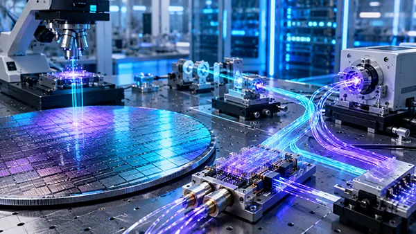
An integrated photonic chip, often called a photonic integrated circuit or PIC, places optical functions on a small semiconductor die in much the same way that an electronic chip combines transistors and wiring. Depending on the design, the photonic section can include modulators that encode electrical data onto light, waveguides that route the light, filters that separate wavelengths and photodetectors that convert incoming light back into electrical signals. Silicon photonics is especially attractive for data-centre use because many of these structures can be produced with manufacturing methods related to conventional semiconductor fabrication. The optical chip does not normally replace the CPU or GPU. Its job is to improve communication around those processors, reducing the distance that very high-speed electrical signals must travel before they are converted to light.
There are several levels of integration. Traditional pluggable optical transceivers sit at the edge of a network switch and connect to the switch chip through electrical traces on the circuit board. Co-packaged optics, usually shortened to CPO, moves the optical engines much closer to the switch ASIC inside the same package area. This shortens the difficult high-speed electrical path and can remove some of the signal-processing overhead used by pluggable modules. Optical I/O goes a step further by bringing photonic links close to CPUs, GPUs or other accelerators, potentially allowing processor-to-processor and processor-to-memory traffic to leave a package as light. These approaches solve related problems, but they are not identical, and data centres are likely to use several of them at the same time for different distances and cost targets.
Intel’s Optical Compute Interconnect work shows how close optical I/O can move to compute silicon. Its first-generation OCI chiplet supports up to 4 Tbps of bidirectional data transfer and is designed to be co-packaged with CPUs, GPUs, IPUs and other system-on-chips. Intel also states that its wider silicon-photonics manufacturing base has shipped more than eight million photonic integrated circuits containing over 32 million on-chip lasers in data-centre transceivers. Those figures matter because the challenge is not only proving that optical I/O works in a laboratory; it is manufacturing lasers, modulators, detectors, packaging and fibre connections with the reliability expected in large data centres. The direction is clear: photonics is moving closer to compute, but commercial adoption depends as much on manufacturing maturity and serviceability as on raw bandwidth.
Where Integrated Photonics Is Appearing in AI Data Centres in 2026
One of the clearest 2026 examples is NVIDIA’s Spectrum-X Ethernet Photonics. NVIDIA announced its silicon-photonics switches in 2025 and said in May 2026 that Spectrum-X Ethernet Photonics had entered production as part of the Vera Rubin generation of AI infrastructure. The design uses co-packaged optics so that optical engines sit close to the switching silicon instead of relying entirely on conventional pluggable transceivers. NVIDIA’s announced configurations include switches with 100 Tbps of total bandwidth and larger designs reaching 400 Tbps, with 800 Gb/s and 200 Gb/s port options. The company has also claimed substantial gains in network power efficiency and resilience compared with traditional optical arrangements. Those figures are vendor measurements rather than universal results for every data-centre design, but the production status is significant because it shows that co-packaged silicon photonics has moved beyond demonstrations into equipment intended for large AI deployments.
Broadcom is following a similar path from the Ethernet switching side. Its Tomahawk 6 family, capable of 102.4 Tbps of switching capacity on a single switch chip, entered production-volume shipments in March 2026. Broadcom has also developed a co-packaged version known as Tomahawk 6 Davisson, which integrates optical engines with the switch package and uses 200 Gb/s optical channels. The company began sampling that CPO device to early-access customers and partners in 2025 while continuing development towards higher per-channel rates. The important point is not which supplier has the largest number on a specification sheet. A 100-Tbps-class switch creates an enormous amount of traffic at its physical edges, and moving that traffic through conventional board-level electrical paths becomes increasingly expensive in power and signal integrity. CPO is being adopted because it tackles that physical problem directly.
Reliability data is also beginning to matter more than laboratory speed records. In 2025 Broadcom reported results from a Meta evaluation covering one million cumulative 400G-equivalent port device hours without a link flap in the tested CPO setup. The same release stated that the CPO design reduced optics power by 65 per cent compared with a pluggable-module solution used for comparison. As with any supplier-published result, the figure should be read in the context of that specific hardware and test environment, not treated as a guaranteed saving for every installation. Even so, it addresses a long-standing concern about placing optics closer to expensive switch silicon: operators need to know that integrated optical engines can remain stable and maintainable for years. By 2026, the conversation is therefore shifting from whether silicon photonics can achieve high bandwidth to how reliably and economically it can be deployed at scale.
Why AI Training and Inference Benefit from Optical Links
Distributed AI workloads create unusually demanding traffic patterns. During model training, accelerators may repeatedly exchange gradients or other updates so that thousands of processors remain synchronised. Some modern models also route different pieces of a request to different groups of processors, creating bursts of traffic that cross the network many times during a single job. If a link is congested, unstable or slow to recover from an error, processors elsewhere in the job may have to wait. That makes network performance part of effective compute performance. Higher-bandwidth optical links can help keep more data moving between racks and switches without requiring proportionally more electrical power at every hop. The practical benefit is not that photons make the mathematical operations inside a GPU faster; it is that the GPU is more likely to receive the data it needs without long communication stalls.
Power is just as important as bandwidth. Large AI facilities are often constrained by how much electricity they can deliver to each rack or building, and every watt used by networking equipment is a watt that cannot be used for additional computation, storage or cooling. At high link speeds, the power consumed by transceivers, retimers and signal-processing electronics can add up across thousands of ports. Moving optical conversion closer to the switch ASIC can reduce the electrical distance and remove some of that overhead. The saving at a single link may appear modest beside a high-power accelerator, but the network contains many links and operates continuously. Lower networking power can also reduce local heat around switch faceplates and boards, although CPO creates its own thermal-design requirements because optical engines now sit closer to hot switching silicon.
Latency improvements require a more careful explanation. Fibre does not provide a magical reduction in propagation time over a few centimetres, and converting signals between electrical and optical forms introduces its own delay. The advantage of integrated photonics is often that it can simplify the high-speed signal path and reduce the need for extra retiming or digital processing stages. In tightly synchronised AI jobs, consistency can be as important as the minimum possible latency: a small number of delayed packets or unstable links can hold back a much larger group of accelerators. This is why suppliers increasingly discuss resilience, signal integrity and sustained application runtime alongside bandwidth. Optical networking can support faster AI work when it reduces the communication overhead around the compute engines, not because light changes the speed of the arithmetic itself.

What Still Limits Wider Adoption of Integrated Photonics
The first major challenge is packaging. Electronic chips can tolerate some variation in ordinary board assembly, but optical components must couple light efficiently into waveguides and fibres that are only micrometres across. Alignment, fibre attachment, sealing, testing and yield all affect cost. A photonic design that performs well on a test bench is not enough if it is difficult to assemble in large volumes or if too many packages fail final inspection. Co-packaged optics also combines components with different manufacturing requirements: high-performance switching silicon, photonic dies, electrical interfaces, fibre connections and laser sources must work together as one system. This is why companies such as NVIDIA, Broadcom, TSMC, Coherent, Lumentum and specialised packaging suppliers are building supply chains around photonics rather than treating it as a single-chip problem.
Thermal management and maintenance are equally practical concerns. A switch ASIC handling tens or hundreds of terabits per second can generate substantial heat, while lasers and some optical components perform best within controlled temperature ranges. Designers therefore have to place photonics close enough to shorten the electrical path without exposing it to unacceptable thermal conditions. Serviceability changes as well. With a conventional pluggable transceiver, a technician can replace one module at the front of the switch. If optical engines are closely integrated with the switch package, replacing a failed component may be more complicated. CPO designs address this in different ways, including external or field-replaceable laser modules and modular fibre connections. The engineering goal is to gain the electrical efficiency of close integration without turning a minor optical fault into an expensive switch replacement.
Cost, interoperability and deployment habits will slow any immediate changeover. Data centres already have large inventories of pluggable optics, established cabling procedures and technicians trained around familiar modules. Ethernet and InfiniBand equipment must also interoperate across generations, suppliers and link types. New photonic hardware therefore has to offer a clear operational advantage rather than merely proving that it is technically elegant. This is one reason the transition is likely to be gradual. Pluggable optics can remain the sensible choice for many links, linear optics can reduce power in selected cases, CPO can serve the highest-bandwidth switches, and optical I/O can move towards processor packages where electrical reach becomes a more serious limit. Integrated photonics is not a single replacement technology; it is a set of tools that will be applied where bandwidth, distance and power justify the added integration.
What the Next Stage of Light-Based Data Movement Is Likely to Look Like
The most realistic near-term change is that optical conversion will continue moving closer to the chips that generate the traffic. Data centres already use fibre extensively between switches and racks. CPO shortens the remaining electrical path inside the switch, while optical I/O aims to shorten it around processors and accelerators. As 200 Gb/s electrical lanes become common in the fastest networking equipment and future designs push beyond them, maintaining long board traces becomes increasingly difficult. This gives photonics a strong reason to move inward. The transition will not happen at the same pace everywhere: hyperscale AI clusters have the strongest incentive because they combine enormous bandwidth demand with strict power limits, while smaller installations may continue using conventional electrical and pluggable optical links for much longer.
It is also important to separate optical interconnects from the more ambitious idea of optical computing. Most integrated photonics entering AI data centres today is designed to move information, not to replace the electronic circuits performing matrix multiplication, control logic or memory operations. Research groups and specialist companies are developing photonic computing techniques, but mainstream AI hardware in 2026 still relies overwhelmingly on electronic GPUs, accelerators and memory. The immediate commercial value of photonics is therefore easier to understand: keep the existing compute engines fed with data more efficiently. That can raise useful system performance without requiring every part of the computing stack to be redesigned around light.
For data-centre operators, the key measure will be system-level efficiency rather than any single record for optical bandwidth. Useful questions include how many watts are required per transmitted bit, how much switch bandwidth fits into a rack, how often links fail, how easily optical parts can be serviced and how much time accelerators spend waiting for the network. The strongest evidence in 2026 is coming from production switches, large-scale reliability testing and deeper investment in optical manufacturing capacity. Integrated photonics will not remove every bottleneck in AI infrastructure, but it directly addresses one of the hardest: moving enormous quantities of data without allowing interconnect power and signal loss to consume an ever larger share of the system budget. That makes light-based I/O a practical part of the next generation of data-centre design rather than a distant replacement for electronics.